Powering the NVM and Embedded Chip Security Technologies
Stephen Las Marias, EE Times Asia
In today’s era of the Internet of Everything (IoE), especially with the proliferation of artificial intelligence (AI), which in turn has ushered in the Artificial Intelligence of Things (AIoT) trend, chip design demands have further intensified. Not only do advanced, high-end applications require powerful CPU cores for processing, but also an increased demand for memory—modern chips need the capability to store critical information, even when powered off.
“With the push toward higher performance and power efficiency, devices like mobile phones, laptops, and cloud data centers increasingly rely on advanced process chips,” says Michael Ho, President of eMemory Technology Inc., during an interview with EE Times Asia. “Today’s applications, especially in HPC (high-performance computing] and AI, demand powerful chips capable of processing large volumes of data and images with enhanced speed and efficiency.”
eMemory is one of the leading providers of non-volatile memory (NVM) IP. “At eMemory, we focus on multimemory development. Our product line includes OTP [one-time programmable], which includes a floating-gate type NeoBit and the antifuse type NeoFuse; MTP [multiple-time programmable], where we have NeoEE and NeoMTP; and we are also providing a PUF-based security solution and our own embedded flash, NeoFlash,” explains Ho.
However, Ho notes that as process shrinks, challenges arise in both process and chip architecture, requiring adjustments to maintain performance, such as controlling electron flow and preventing leakage, which can impact power efficiency and reliability.
“ To meet the demands of advanced applications, it is essential to extend our NVM capabilities to advanced processes. However, these processes are highly complex, making it impractical to tailor them to perfectly align with the design of every individual component.” explains Ho. “Our engineers have to find different kind of ways—from device level to design level—to achieve a very reliable and robust NVM technology in those advanced process nodes.”
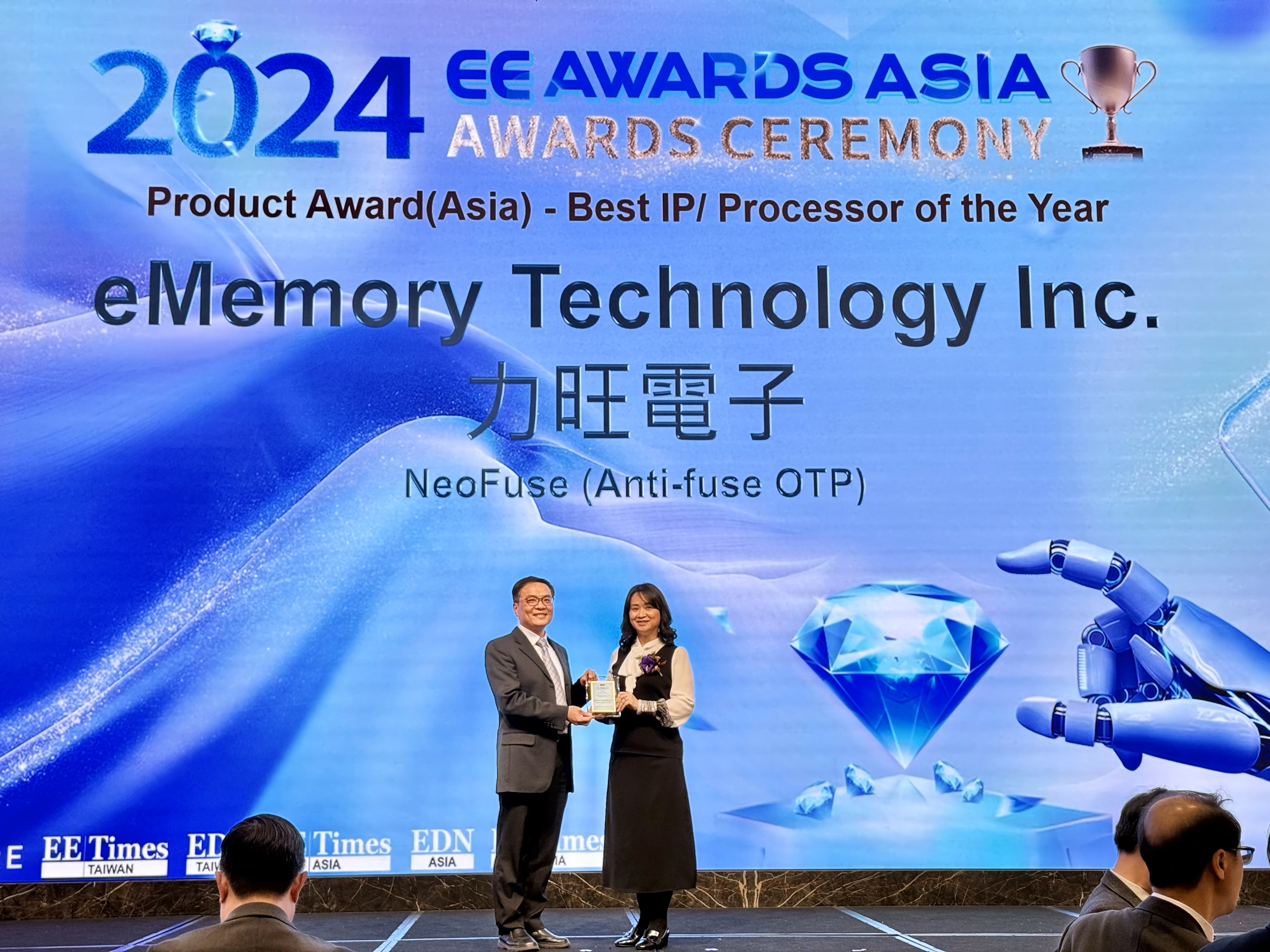
NeoFuse, eMemory’s advanced anti-fuse OTP solution and a recipient of the Best IP/Processor of the Year award at EE Awards Asia 2024, solves a key industry challenge: scaling with advanced nodes without increasing cost or design complexity.

“As advanced processes develop to 5nm, the rated supply voltage of a component lows from 1.8V to 1.2V. NeoFuse’s design needed to overcome the challenge of lower power supply while maintaining high programming voltage and performance. NeoFuse uses an innovative circuit that boosts the internal voltage three to four times higher while maintaining reliability of devices. Its new architecture also achieves high temperature tolerance, supporting up to 150°C in sub-5nm processes,” explains Ho.
Additionally, to fulfill the new demand of the advanced applications, eMemory’s NeoFuse reserves parity bits in each word as a standard design, enabling clients to implement Error Correction Code (ECC) schemes to ensure data integrity. This makes it an ideal solution for high-reliability SoC applications, including automotive systems and beyond.
“NeoFuse aims to support all kinds of cutting-edge applications’ advancements,” Ho says.
But what also makes NeoFuse a recipient of an EE Awards is its uniqueness. Compared to eFuse, NeoFuse’s mechanism makes the physical differences between programmed and unprogrammed cells invisible, making it a safer option than eFuse. In addition, when there is a large capacity requirement, the required area (footprint) of NeoFuse is also relatively economical.

“Compared to other OTP, NeoFuse’s patented 3T structure adds a regulating transistor to improve yield, reliability, and programming success compared to traditional 2T designs, which reduces testing time and costs,” says Ho. “Compatible with standard logic processes, NeoFuse supports fast time-to-market, quality, and cost efficiency for leading-edge applications. As an OTP that always passes advanced processes—from 16nm to 3nm—at the first cut, NeoFuse is ideal for demanding applications such as AI, HPC, data centers and automotive fields.”
Meanwhile, when it comes to high-end applications, all chips that require a large amount of computing faces the challenge of a sudden increase in SRAM demand and a decline in yield. To address this issue, eMemory recently cooperated with Siemens on an SRAM repair toolset, which integrates the NeoFuse OTP into Siemens’ Tessent MemoryBIST (Built-in Self-Test) tool, and coupled with the interface design jointly developed by eMemory subsidiary PUFsecurity Corp. to makes the SRAM repair tool easier to use.
“Siemens’ Tessent MemoryBIST has a market share of more than 90%, so, cooperating with Siemens on SRAM Repair is an OTP application trend that we value very much,” says Ho.
Addressing Chip Security Issues
Apart from the increasing complexity of chip designs to address the high-performance requirements and interconnectedness of the latest applications in almost every sector, another critical challenge that designers are intensely focusing on is security.
In the automotive sector, fintech, industrial automation, or even personal devices such as smartphones and portables, chip security has never been more critical amid the increasingly sophisticated cyberattacks. In fact, threat actors can even leverage the use of advanced AI, especially generative AI, to create malicious content to harm devices.
These trends—the need to secure interconnected devices, protect sensitive data across a wide range of applications, the growing urgency to combat cyber risks—bode well for the embedded security industry and its ecosystem. According to research firm MarketsandMarkets, the embedded security market is expected to grow from $7.4 billion in 2023 to around $9.8 billion by 2028—growing at a compound annual growth rate (CAGR) of 5.7% from 2023 to 2028.
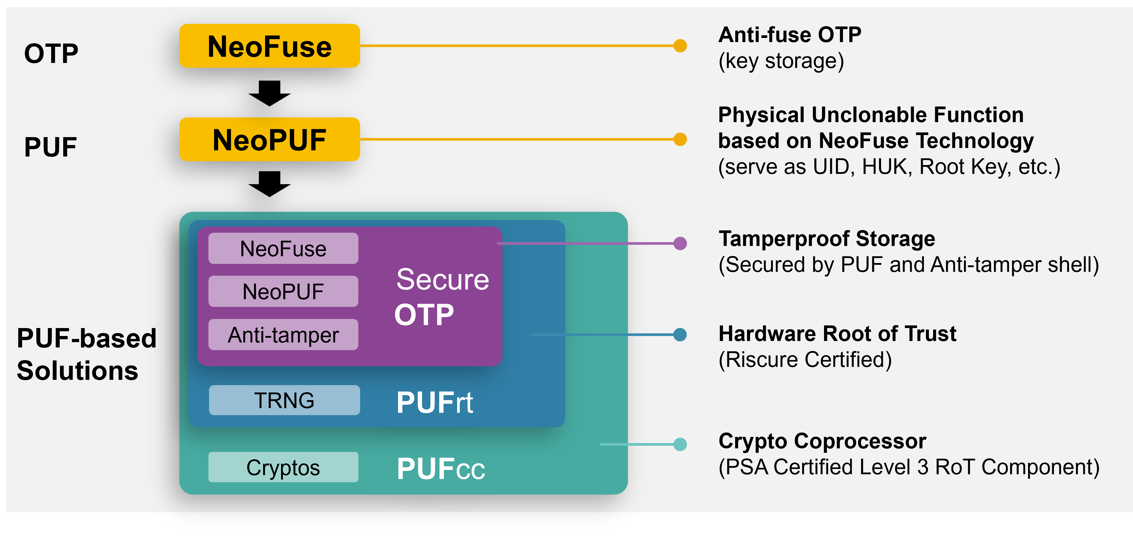
And leading this front is eMemory subsidiary PUFsecurity Corp. eMemory has further invented NeoPUF with nearly ideal PUF performance through NeoFuse technology. Based on its NeoFuse and NeoPUF technologies and industry resources, eMemory established PUFsecurity in 2019, focusing on developing secure storage and key technologies into different levels of hardware security solutions, including the Hardware Root of Trust (PUFrt) and Crypto Coprocessor (PUFcc).
In PUFrt, PUF serves as the core for generating a unique password for each chip, enabling the creation of root keys or unique identification codes (UID), and securely stored in NeoFuse OTP. The True Random Number Generator (TRNG) within PUFrt seamlessly integrates PUF values to produce high-quality random numbers, meeting diverse and stringent security operation needs. The overall design of PUFrt is interlocked to form a robust anti-attack protective shell, establishing a solid foundation for building a trust and security chain from each IoT endpoint chip. On top of PUFrt, PUFcc incorporates a comprehensive suite of encryption algorithms certified by the National Institute of Standards and Technology (NIST), supporting advanced security functions such as secure boot, secure updates, and secure debugging.
By 2023, the company introduced the One-Stop Shop Security Platform to demonstrate a more comprehensive, market-ready secure IP platform with upgraded controllers and interface designs, such as Memory Mapping, Behavioral Models, and Regression Test Methodology support smoother adoption and verification.
“As a group, eMemory and PUFsecurity integrate all security elements to deliver a comprehensive solution for our customers. This unique strength is difficult to replicate, especially since very few companies excel in both hardware and software IP design.” says Ho.

One of the recent developments from PUFsecurity is the recently launched PUFcc7, an upgraded version that meets TLS 1.3’s security requirements, particularly in new cryptos. Also, PUFsecurity and Arm joined forces to demonstrate a powerful security framework combining PUFcc and Arm Corstone-300 and achieved SESIP and PSA Certified Level 3 RoT Component certification in the fourth quarter of this year.
“Many customers have already used our PUFrt with Arm architecture to enhance hardware security. On the other hand, the adoption of PUFcc has also picked up rapidly. Customers have taken the advantage of complete integration and CAVP-certified crypto engines to accelerate products’ time-to-market and certification process,” says Ho.
In fact, as demand for data centers and the cloud has been exploding exponentially, the industry has established Caliptra, an open standard for silicon root of trust targeted at chips designed for data center applications, including CPUs, GPUs, and DPUs.
“For customers who require data center services, their terminal equipment must also comply with Caliptra's specifications,” explains Ho. “Our root of trust solution—PUFrt—is the security required by data center applications. In fact, more and more customers are requesting PUFrt. According to Caliptra documentation, the goal is to first adopt Caliptra in confidential computing, with plans to expand to all chip types. The demand for security solutions driven by relevant regulations is also an opportunity we are quite optimistic about.”
Ho adds that PUFsecurity will keep upgrading and completing its entire security portfolio to offer the industry a one-stop-shop service and innovative solutions, whether the designs, availabilities (150nm–3nm), security framework references, and certifications.
And it is for these reasons that PUFsecurity is a recipient of this year’s Best Security Technology Platform at the EE Awards Asia.

“EE Times is an influential technology media in the industry. It is an honor for us to be the recipient of these awards together with many semiconductor giants. With this kind of affirmation, we will go further. We also hope that through the EE Awards, people who are unfamiliar with eMemory and PUFsecurity will get to know us, and lead to more potential cooperation opportunities,” says Ho.
Next Step Forward
Ho says they will continue to actively expand the roadmap of eMemory IP in process nodes. “We expect that NeoFuse will complete the qualification of 3nm next year, and 2nm will always be included in the plan. In addition, several new technologies are also under development.”
Meanwhile, PUFsecurity is about to launch a brand-new solution, PUFhsm, which is born to fulfil the automotive vertical and enable eight security goals with a CPU-integrated architecture—secure boot, secure update, secure deployment, key management, lifecycle management, secure debugging, secure monitoring, and compliant with the EVITA Full.
“Overall, because our products continue to improve and have been successfully expanded to various technology platforms and advanced process nodes, coupled with the cooperation and promotion with industrial giants, which will accelerate our progress in the advanced application market, we are optimistic about future growth,” Ho concludes.

